Page Not Found
Page not found. Your pixels are in another canvas.

A list of all the posts and pages found on the site. For you robots out there is an XML version available for digesting as well.
Page not found. Your pixels are in another canvas.
About me
This is a page not in th emain menu
Published:
Low excess noise digital alloy APDs
Published:
Linearized ring-assisted Mach–Zehnder interferometers
Published:
Si depeletion mode modulators
Published:
This is a sample blog post. Lorem ipsum I can’t remember the rest of lorem ipsum and don’t have an internet connection right now. Testing testing testing this blog post. Blog posts are cool.
Published:
Quantum dot optical frequency comb
Published:
NRZ eye diagram 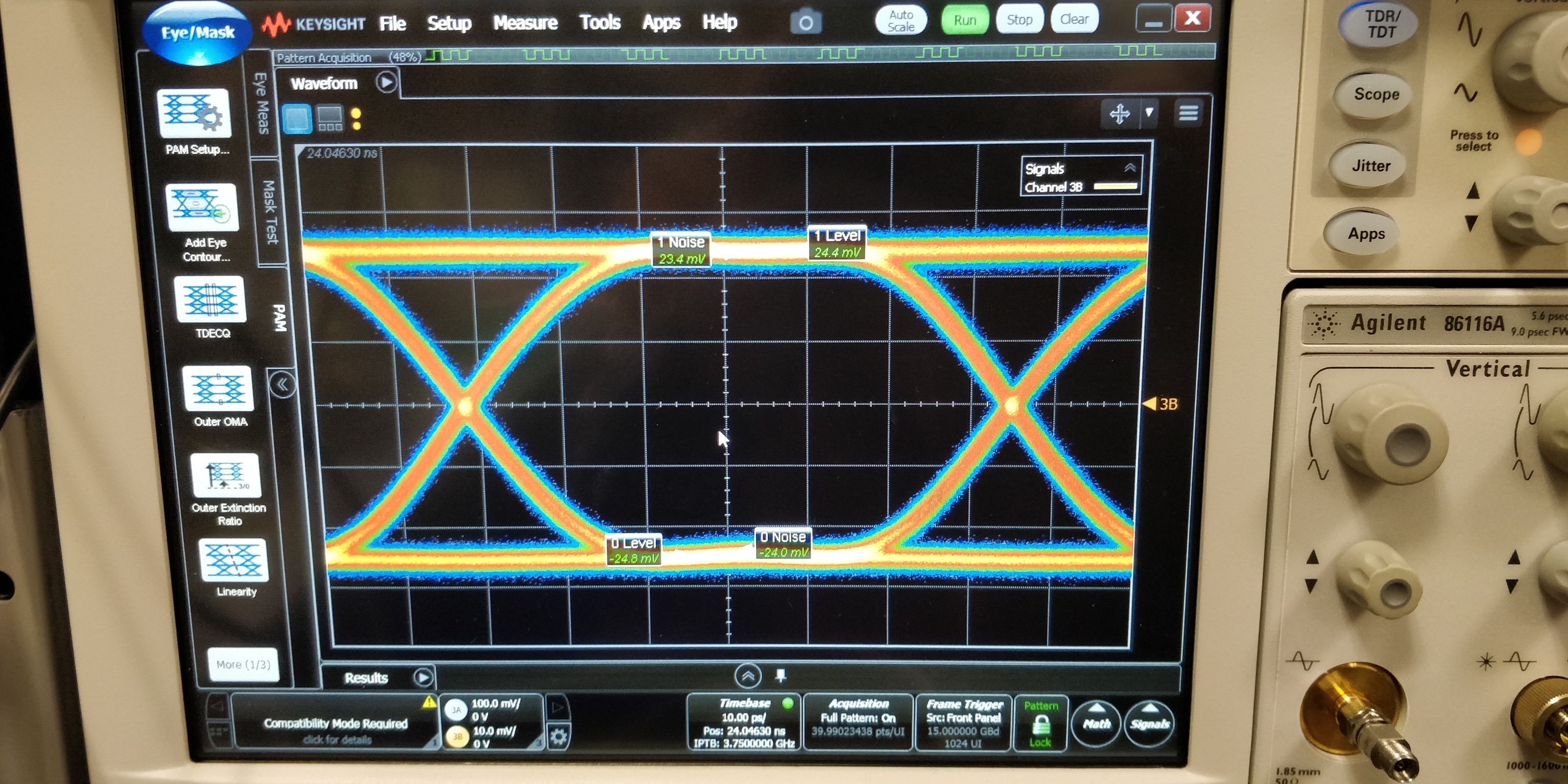
Published in Optics Express, 2017
We report AlxIn1-xAsySb1-y PIN and Separate Absorption, Charge and Multiplication (SACM) avalanche photodiodes (APDs) with high temperature stability. This work is based on measurements of avalanche breakdown voltage of these devices for temperatures between 223 K and 363 K. Breakdown voltage temperature coefficients are shown to be lower than those of APDs fabricated with other materials with comparable multiplication layer thicknesses.
Recommended citation: Jones, Andrew H., Yuan Yuan, Min Ren, Scott J. Maddox, Seth R. Bank, and Joe C. Campbell. "Al x In 1-x As y Sb 1-y photodiodes with low avalanche breakdown temperature dependence." Optics express 25, no. 20 (2017): 24340-24345. https://opg.optica.org/oe/fulltext.cfm?uri=oe-25-20-24340&id=373694
Published in IEEE Photonics Technology Letters, 2018
We report avalanche photodiodes (APDs) fabricated from the digital alloy Al0.8In0.2As0.23Sb0.77 (lattice-matched to GaSb). The APDs exhibit high avalanche multiplication and low excess noise.
Recommended citation: Rockwell, Ann-Katheryn, Yuan Yuan, Andrew H. Jones, Stephen D. March, Seth R. Bank, and Joe C. Campbell. "Al 0.8 In 0.2 As 0.23 Sb 0.77 Avalanche Photodiodes." IEEE Photonics Technology Letters 30, no. 11 (2018): 1048-1051. https://ieeexplore.ieee.org/document/8338119
Published in Journal of Lightwave Technology, 2018
InAlAs digital alloy avalanche photodiodes exhibit lower excess noise than those fabricated from conventional random alloy material. Experiment and Monte Carlo simulation both show that relative to the random alloy the ionization probability for electrons is slightly lower while that of holes is greatly suppressed. We propose that the suppression of carrier ionization probability in digital alloys happens because of the creation of minibands that localize carriers. The difference of suppression between conduction bands and valence bands comes from the difference of scattering path.
Recommended citation: Zheng, Jiyuan, Yuan Yuan, Yaohua Tan, Yiwei Peng, Ann K. Rockwell, Seth R. Bank, Avik W. Ghosh, and Joe C. Campbell. "Digital alloy InAlAs avalanche photodiodes." Journal of Lightwave Technology 36, no. 17 (2018): 3580-3585. https://opg.optica.org/oe/fulltext.cfm?uri=oe-25-20-24340&id=373694
Published in Photonics Research, 2018
Digital alloy In0.52Al0.48As avalanche photodiodes exhibit lower excess noise than those fabricated from random alloys. This paper compares the temperature dependence, from 203 to 323 K, of the impact ionization characteristics of In0.52Al0.48As and Al0.74Ga0.26As digital and random alloys. These results provide insight into the low excess noise exhibited by some digital alloy materials, and these materials can even obtain lower excess noise at low temperature.
Recommended citation: Yuan, Yuan, Jiyuan Zheng, Yaohua Tan, Yiwei Peng, Ann-Kathryn Rockwell, Seth R. Bank, Avik Ghosh, and Joe C. Campbell. "Temperature dependence of the ionization coefficients of InAlAs and AlGaAs digital alloys." Photonics Research 6, no. 8 (2018): 794-799. https://opg.optica.org/prj/fulltext.cfm?uri=prj-6-8-794&id=395329
Published in Applied Physics Letters, 2018
Over the past 40+ years, III-V materials have been intensively studied for avalanche photodetectors, driven by applications including optical communications, imaging, quantum information processing, and autonomous vehicle navigation. Unfortunately, impact ionization is a stochastic process that introduces noise, thereby limiting sensitivity and achievable bandwidths, leading to intense effort to mitigate this noise through the identification of different materials and device structures. Exploration of these materials has seen limited success as it has proceeded in a largely ad hoc fashion due to little consensus regarding which fundamental properties are important. Here, we report an exciting step toward deterministic design of low-noise avalanche photodetector materials by alternating the composition at the monolayer scale; this represents a dramatic departure from previous approaches, which have concentrated on either unconventional compounds/alloys or nanoscale band-engineering. In particular, we demonstrate how to substantially improve upon the noise characteristics of the current state-of-the art telecom avalanche multipliers, In0.52Al0.48As grown on InP substrates, by growing the structure as a strain-balanced digital alloy of InAs and AlAs layers, each only a few atomic layers thick. The effective k-factor, which has historically been considered a fundamental material property, was reduced by 6–7× from k = 0.2 for bulk In0.52Al0.48As to k = 0.05 by using the digital alloy technique. We also demonstrate that these “digital alloys” can significantly extend the photodetector cutoff wavelength well beyond those of their random alloy counterparts.
Recommended citation: Rockwell, A. K., M. Ren, M. Woodson, A. H. Jones, S. D. March, Y. Tan, Y. Yuan et al. "Toward deterministic construction of low noise avalanche photodetector materials." Applied Physics Letters 113, no. 10 (2018): 102106. https://aip.scitation.org/doi/10.1063/1.5040592
Published in IEEE Photonics Technology Letters, 2019
Digital alloy AlInAsSb avalanche photodiodes exhibit low excess noise comparable to those fabricated from Si. The electron and hole ionization coefficients are critical parameters for simulation and analysis of high-sensitivity receivers. We report ionization coefficients using a mixed injection technique that employs measurement of the gain for different incident wavelengths and a simulation algorithm.
Recommended citation: Yuan, Yuan, Jiyuan Zheng, Ann K. Rockwell, Stephen D. March, Seth R. Bank, and Joe C. Campbell. "AlInAsSb impact ionization coefficients." IEEE Photonics Technology Letters 31, no. 4 (2019): 315-318. https://ieeexplore.ieee.org/document/8620234
Published in Journal of Lightwave Technology, 2019
We report Al0.7InAsSb avalanche photodiodes grow as ternary-binary and binary-binary digital alloys. Their characteristics of ideality factor, activation energy, temperature-dependent excess noise, temperature stability, and impact ionization coefficients are compared.
Recommended citation: Yuan Yuan, Ann Kathryn Rockwell, Yiwei Peng, Jiyuan Zheng, Stephen D March, Andrew H Jones, Min Ren, Seth R Bank, and Joe C Campbell. "Comparison of Different Period Digital Alloy AlInAsSb Avalanche Photodiodes." Journal of Lightwave Technology 37, no. 14 (2019): 3647-3654. https://opg.optica.org/abstract.cfm?uri=jlt-37-14-3647
Published in physica status solidi (RRL)-Rapid Research Letters, 2019
The optical absorption characteristics of the InAlAs digital alloy semiconductor are investigated. The external quantum efficiency of the InAlAs digital alloy is compared with that of the In0.52Al0.48As random alloy. Unlike the random alloy, the digital alloy exhibits electric?field?induced Stark localization, which increases the optical absorption and suppresses the Franz-Keldysh red shift of the optical absorption edge.
Recommended citation: Yuan Yuan, Jiyuan Zheng, Keye Sun, Andrew H Jones, Ann K Rockwell, Stephen D March, Yang Shen, Seth R Bank, and Joe C Campbell. "Stark-Localization-Limited Franz-Keldysh effect in InAlAs Digital Alloys." physica status solidi (RRL)-Rapid Research Letters 13, no. 9 (2019): 1900272. https://onlinelibrary.wiley.com/doi/abs/10.1002/pssr.201900272
Published in Journal of Applied Physics, 2019
InAlAs digital alloy avalanche photodiodes (APDs) exhibit lower noise than their random alloy counterparts. The electronic dispersion properties of digital alloy materials are unique, creating minigaps in their valence band structure. In this paper, we use computational models with environment-dependent tight-binding parameters to calculate the electronic dispersion properties of InAlAs digital alloys with various stacking directions, stacking modes, and periods, which can provide guidance for optimizing the structure of InAlAs digital alloy APDs.
Recommended citation: Zheng, J., Y. Tan, Y. Yuan, A. W. Ghosh, and J. C. Campbell. "Tuning of energy dispersion properties in InAlAs digital alloys." Journal of Applied Physics 125, no. 24 (2019): 245702. https://aip.scitation.org/doi/abs/10.1063/1.5091694
Published in Optics letters, 2019
We demonstrate a III-V avalanche photodiode (APD) grown by heteroepitaxy on silicon. This InGaAs/InAlAs APD exhibits low dark current, gain >20, external quantum efficiency >40%, and similar low excess noise, k~0.2, as InAlAs APDs on InP.
Recommended citation: Yuan Yuan, Daehwan Jung, Keye Sun, Jiyuan Zheng, Andrew H Jones, John E Bowers, and Joe C Campbell. "III-V on silicon avalanche photodiodes by heteroepitaxy." Optics letters 44, no. 14 (2019): 3538-3541. https://opg.optica.org/abstract.cfm?uri=ol-44-14-3538
Published in Optics Express, 2019
The dark current of a photodetector is a key parameter for high-sensitivity optical receivers. We report low-dark-current, triple-mesa avalanche photodiodes that have ~50 times lower dark current than conventional single-mesa devices, and suppress surface leakage. The tolerances of triple-mesa avalanche photodiode parameters are presented.
Recommended citation: Yuan Yuan, Yabo Li, Joshua Abell, JiYuan Zheng, Keye Sun, Christopher Pinzone, and Joe C Campbell. "Triple-mesa avalanche photodiodes with very low surface dark current." Optics Express 27, no. 16 (2019): 22923-22929. https://opg.optica.org/abstract.cfm?uri=oe-27-16-22923
Published in Applied Physics Letters, 2019
3D band structure-based Monte Carlo simulations have been utilized to simulate InAlAs digital alloy avalanche photodiodes. The simulated current–voltage curve and excess noise factor fit well with experimental results. Ionization coefficients calculated by the Monte Carlo technique were incorporated into the recurrence model, which is easier to implement and requires less computation time.
Recommended citation: Zheng, J., Y. Yuan, Y. Tan, Y. Peng, A. Rockwell, S. R. Bank, A. W. Ghosh, and J. C. Campbell. "Simulations for InAlAs digital alloy avalanche photodiodes." Applied Physics Letters 115, no. 17 (2019): 171106. https://aip.scitation.org/doi/10.1063/1.5114918
Published in IEEE Photonics Technology Letters, 2019
Recommended citation: Jones, Andrew H., Ann-Kathryn Rockwell, Stephen D. March, Yuan Yuan, Seth R. Bank, and Joe C. Campbell. "High Gain, Low Dark Current Al 0.8 In 0.2 As 0.23 Sb 0.77 Avalanche Photodiodes." IEEE Photonics Technology Letters 31, no. 24 (2019): 1948-1951. https://ieeexplore.ieee.org/document/8892636
Published in Journal of Applied Physics , 2019
Recently, InAlAs digital alloys have been shown to exhibit unique electronic dispersion properties, which can be used to make low-noise avalanche photodiodes. In this paper, the strain effect is analyzed for its impact on the band structure of the InAlAs digital alloy. Simulation using a tight binding model that includes the strain effect yields bandgap energies that are consistent with experimental results. The bandgap would be larger without strain. In addition, a positive relationship has been found between minigaps of the InAlAs digital alloy and the band offset between bulk InAs and AlAs at the same position in k-space.
Recommended citation: Zheng, J., Y. Tan, Y. Yuan, A. W. Ghosh, and J. C. Campbell. "Strain effect on band structure of InAlAs digital alloy." Journal of Applied Physics 125, no. 8 (2019): 082514. https://aip.scitation.org/doi/abs/10.1063/1.5045476
Published in Applied Physics Letters, 2019
Recommended citation: Shen, Yang, Andrew H. Jones, Yuan Yuan, Jiyuan Zheng, Yiwei Peng, Brenda VanMil, Kimberley Olver et al. "Near ultraviolet enhanced 4H-SiC Schottky diode." Applied Physics Letters 115, no. 26 (2019): 261101. https://aip.scitation.org/doi/10.1063/1.5129375
Published in InfoMat, 2020
Avalanche photodiodes fabricated from AlInAsSb grown as a digital alloy exhibit low excess noise. In this article, we investigate the band structure-related mechanisms that influence impact ionization. Band-structures calculated using an empirical tight-binding method and Monte Carlo simulations reveal that the mini-gaps in the conduction band do not inhibit electron impact ionization. Good agreement between the full band Monte Carlo simulations and measured noise characteristics is demonstrated.
Recommended citation: Zheng, Jiyuan, Sheikh Z. Ahmed, Yuan Yuan, Andrew Jones, Yaohua Tan, Ann K. Rockwell, Stephen D. March, Seth R. Bank, Avik W. Ghosh, and Joe C. Campbell. "Full band Monte Carlo simulation of AlInAsSb digital alloys." InfoMat 2, no. 6 (2020): 1236-1240. https://onlinelibrary.wiley.com/doi/full/10.1002/inf2.12112
Published in Journal of Lightwave Technology, 2020
A Si-Ge waveguide avalanche photodiode with extremely high temperature stability is demonstrated. The breakdown voltage increases ~4.2 mV/C, bandwidth reduces ~0.09%/C, and gain-bandwidth product reduces ~0.24%/C with temperature increased from 30 C to 90 C. Additionally, it maintains superior performance with low breakdown voltage of ~10 V, high multiplication gain of >15, high bandwidth of ~24.6 GHz, high gain-bandwidth product of >240 GHz, high internal quantum efficiency of ~100%, and clear eye diagrams with 64 Gbps PAM4 modulation at 90 C.
Recommended citation: Yuan Yuan, Zhihong Huang, Binhao Wang, Wayne V Sorin, Xiaoge Zeng, Di Liang, Marco Fiorentino, Joe C Campbell, and Raymond G Beausoleil. "64 Gbps PAM4 Si-Ge waveguide avalanche photodiodes with excellent temperature stability." Journal of Lightwave Technology 38, no. 17 (2020): 4857-4866. https://opg.optica.org/abstract.cfm?uri=jlt-38-17-4857
Published in Photonics Research, 2020
We demonstrate low-voltage waveguide silicon-germanium avalanche photodiodes (APDs) integrated with distributed Bragg reflectors (DBRs). The internal quantum efficiency is improved from 60% to 90% at 1550 nm assisted with DBRs while still achieving a 25 GHz bandwidth. A low breakdown voltage of 10 V and a gain bandwidth product of near 500 GHz are obtained. APDs with DBRs at a data rate of 64 Gb/s pulse amplitude modulation with four levels (PAM4) show a 30% - 40% increase in optical modulation amplitude (OMA) compared to APDs with no DBR. A sensitivity of around -13 Bm at a data rate of 64 Gb/s PAM4 and a bit error rate of 2.4x10^-4 is realized for APDs with DBRs, which improves the sensitivity by ~2 B compared to APDs with no DBR.
Recommended citation: Wang, Binhao, Zhihong Huang, Yuan Yuan, Di Liang, Xiaoge Zeng, Marco Fiorentino, and Raymond G. Beausoleil. "64 Gb/s low-voltage waveguide SiGe avalanche photodiodes with distributed Bragg reflectors." Photonics Research 8, no. 7 (2020): 1118-1123. https://opg.optica.org/prj/fulltext.cfm?uri=prj-8-7-1118&id=432418
Published in IEEE Journal of Lightwave Technology , 2021
III-V material based digital alloy Avalanche Photodiodes (APDs) have recently been found to exhibit low noise similar to Silicon APDs. The III-V materials can be chosen to operate at any wavelength in the infrared spectrum. In this work, we present a physics-based SPICE compatible compact model for APDs built from parameters extracted from an Environment-Dependent Tight Binding (EDTB) model calibrated to ab-initio Density Functional Theory (DFT) and Monte Carlo (MC) methods. Using this approach, we can accurately capture the physical characteristics of these APDs in integrated photonics circuit simulations.
Recommended citation: Ahmed, Sheikh Z., Samiran Ganguly, Yuan Yuan, Jiyuan Zheng, Yaohua Tan, Joe C. Campbell, and Avik W. Ghosh. "A physics based multiscale compact model of pin avalanche photodiodes." Journal of Lightwave Technology 39, no. 11 (2021): 3591-3598. https://ieeexplore.ieee.org/document/9383842
Published in IEEE Journal of Selected Topics in Quantum Electronics, 2021
We present a loop reflector-assisted silicon-germanium waveguide avalanche photodiode with improved responsivity. Compared to the same APD without the reflector, it has 1.49 times higher responsivity, ~1.12 A/W, without compromising the speed performance. It exhibits a 3 dB-bandwidth of ~25 GHz, a build-up time limited gain-bandwidth product of ~296 GHz, a highest gain-bandwidth product of ~497 GHz. Clear eye diagrams are measured at both 32 Gbps NRZ and 64 Gbps PAM4 modulation, and a 1~2 dB better sensitivity up to -15.7 dBm with 32 Gbps NRZ at a BER of 2.4e-4.
Recommended citation: Yuan Yuan, Zhihong Huang, Xiaoge Zeng, Di Liang, Wayne V Sorin, Marco Fiorentino, and Raymond G Beausoleil. "High responsivity Si-Ge waveguide avalanche photodiodes enhanced by loop reflector." IEEE Journal of Selected Topics in Quantum Electronics 28, no. 2 (2021): 1-8. https://ieeexplore.ieee.org/abstract/document/9448380/
Published in arXiv preprint , 2021
Simple analytical expressions for estimation of second order output intercept point (OIP2) and third order output intercept point (OIP3) of surface normal uni-traveling carrier (UTC) and modified uni-traveling carrier (MUTC) photodiode (PD) are derived. These equations are valuable for estimation of OIP for high power (M)UTC-PDs during the design phase.
Recommended citation: Sun, Keye, Junyi Gao, Yuan Yuan, Joe Campbell, and Andreas Beling. "Simple Formulas for Output Interception Power Estimation of Uni-Traveling Carrier Photodiodes." arXiv preprint: 2108.07230 (2021). https://arxiv.org/abs/2108.07230
Published in Advanced Intelligent Systems , 2021
3D sensing is a primitive function that allows imaging with depth information generally achieved via the time-of-flight (ToF) principle. However, time-to-digital converters (TDCs) in conventional ToF sensors are usually bulky, complex, and exhibit large delay and power loss. To overcome these issues, a resistive time-of-flight (R-ToF) sensor that can measure the depth information in an analog domain by mimicking the biological process of spike-timing-dependent plasticity (STDP) is proposed herein. The R-ToF sensors based on integrated avalanche photodiodes (APDs) with memristive intelligent matters achieve a scan depth of up to 55 cm (89% accuracy and 2.93 cm standard deviation) and low power consumption (0.5 nJ/step) without TDCs. The in-depth computing is realized via R-ToF 3D imaging and memristive classification. This R-ToF system opens a new pathway for miniaturized and energy-efficient neuromorphic vision engineering that can be harnessed in light-detection and ranging (LiDAR), automotive vehicles, biomedical in vivo imaging, and augmented/virtual reality.
Recommended citation: Park, Minseong, Yuan Yuan, Yongmin Baek, Andrew H. Jones, Nicholas Lin, Doeon Lee, Hee Sung Lee, Sihwan Kim, Joe C. Campbell, and Kyusang Lee. "Neuron-Inspired Time-of-Flight Sensing via Spike-Timing-Dependent Plasticity of Artificial Synapses." Advanced Intelligent Systems 4, no. 3 (2022): 2100159. https://onlinelibrary.wiley.com/doi/full/10.1002/aisy.202100159
Published in Electronics, 2022
All-silicon microring resonator photodiodes are attractive for silicon photonics integrated circuits due to their compactness, wavelength division multiplexing ability, and the absence of germanium growth. To analyze and evaluate the performance of the microring photodiode, we derived closed-form expression of the response transfer function with both electrical and optical behavior included, using a small-signal analysis. The thermo-optic nonlinearity resulting from optical loss and ohmic heating was simulated and considered in the model. The predicted response achieved close agreement with the experiment results, which provides an intuitive understanding of device performance. We analytically investigated the responsivity-bandwidth product and demonstrated that the performance is superior when the detuning frequency is zero.
Recommended citation: Peng, Yiwei, Wayne V. Sorin, Stanley Cheung, Yuan Yuan, Zhihong Huang, Marco Fiorentino, and Raymond G. Beausoleil. "Small-Signal Analysis of All-Si Microring Resonator Photodiode." Electronics 11, no. 2 (2022): 183. https://www.mdpi.com/2079-9292/11/2/183
Published in Photonics Research, 2022
We discuss the design and demonstration of various III-V/Si asymmetric Mach-Zehnder interferometer (AMZI) and ring-assisted AMZI (de-) interleavers operating at O-band wavelengths with 65 GHz channel spacing. The wafer-bonded III-V/Si metal-oxide-semiconductor capacitor (MOSCAP) structure facilitates ultra-low-power phase tuning on a heterogeneous platform that allows for complete monolithic transceiver photonic integration. The second- and third-order MOSCAP AMZI (de-) interleavers exhibit cross-talk (XT) levels down to -22 dB and -32 dB with tuning power of 83.0 nW and 53.0 nW, respectively. The one-, two-, and three-ring-assisted MOSCAP AMZI (de-) interleavers have XT levels down to -27 dB, -22 dB, and -20 dB for tuning power of 10.0 nW, 7220.0 nW, and 33.6 nW, respsectively. The leakage current density is measured to be in the range of 1.6 ~ 27 uA/cm^2. To the best of our knowledge, we have demonstrated for the first time, athermal III-V/Si MOSCAP (de-) interleavers with the lowest XT and reconfiguration power consumption on a silicon platform.
Recommended citation: Cheung, Stanley, Geza Kurczveil, Yingtao Hu, Mingye Fu, Yuan Yuan, Di Liang, and Raymond G. Beausoleil. "Ultra-power-efficient heterogeneous III-V/Si MOSCAP (de-) interleavers for DWDM optical links." Photonics Research 10, no. 2 (2022): A22-A34. https://opg.optica.org/prj/abstract.cfm?uri=prj-10-2-a22
Published in Journal of Semiconductor, 2022
Silicon photonics technology has drawn significant interest due to its potential for compact and high-performance photonic integrated circuits. The Ge-or III-V material-based avalanche photodiodes integrated on silicon photonics provide ideal high sensitivity optical receivers for telecommunication wavelengths. Herein, the last advances of monolithic and heterogeneous avalanche photodiodes on silicon are reviewed, including different device structures and semiconductor systems.
Recommended citation: Yuan Yuan, Bassem Tossoun, Zhihong Huang, Xiaoge Zeng, Geza Kurczveil, Marco Fiorentino, Di Liang, and Raymond G Beausoleil. "Avalanche photodiodes on silicon photonics." (2022). https://iopscience.iop.org/article/10.1088/1674-4926/43/2/021301/meta
Published in IEEE Photonics Technology Letters, 2022
We investigate the bit error rates and eye diagrams of Si-Ge avalanche photodiodes at 32 Gb/s NRZ for different optical signal-to-noise ratios. The relationship between receiver sensitivity and optical signals quality has been analyzed using theoretical calculation and simulation. This sensitivity analysis provides guidance on signal quality tolerances for the APD-based optical links.
Recommended citation: Yuan Yuan, Sudharsanan Srinivasan, Yiwei Peng, Di Liang, Zhihong Huang, Wayne V Sorin, Stanley Cheung, Marco Fiorentino, and Raymond G Beausoleil. "OSNR Sensitivity Analysis for Si-Ge Avalanche Photodiodes." IEEE Photonics Technology Letters 34, no. 6 (2022): 321-324. https://ieeexplore.ieee.org/abstract/document/9718330/
Published in ACS Photonics, 2022
A compact two-segment depletion mode silicon microring resonator modulator with PAM4 modulation data rate up to 100 Gb/s has been demonstrated. The microring resonator modulator exhibits a free spectrum range of ~5.7 nm, a quality factor of ~3600, a DC extinction ratio of ~13 dB, an electro-optical phase shift efficiency VpiL of ~1 Vcm, and an electro-optical bandwidth of ~40 GHz.
Recommended citation: Yuan Yuan, Wayne V Sorin, Zhihong Huang, Xiaoge Zeng, Di Liang, Ankur Kumar, Samuel Palermo, Marco Fiorentino, and Raymond G Beausoleil. "A 100 Gb/s PAM4 Two-Segment Silicon Microring Resonator Modulator Using a Standard Foundry Process." ACS Photonics 9, no. 4 (2022): 1165-1171. https://pubs.acs.org/doi/abs/10.1021/acsphotonics.1c01389
Published in Nature Communications, 2022
One of the most common approaches for quenching single-photon avalanche diodes is to use a passive resistor in series with it. A drawback of this approach has been the limited recovery speed of the single-photon avalanche diodes. High resistance is needed to quench the avalanche, leading to slower recharging of the single-photon avalanche diodes depletion capacitor. We address this issue by replacing a fixed quenching resistor with a bias-dependent adaptive resistive switch. Reversible generation of metallic conduction enables switching between low and high resistance states under unipolar bias. As an example, using a Pt/Al2O3/Ag resistor with a commercial silicon single-photon avalanche diodes, we demonstrate avalanche pulse widths as small as ~ 30?ns, 10x smaller than a passively quenched approach, thus significantly improving the single-photon avalanche diodes frequency response. The experimental results are consistent with a model where the adaptive resistor dynamically changes its resistance during discharging and recharging the single-photon avalanche diodes.
Recommended citation: Zheng, Jiyuan, Xingjun Xue, Cheng Ji, Yuan Yuan, Keye Sun, Daniel Rosenmann, Lai Wang, Jiamin Wu, Joe C. Campbell, and Supratik Guha. "Dynamic-quenching of a single-photon avalanche photodetector using an adaptive resistive switch." Nature Communications 13, no. 1 (2022): 1-12. https://www.nature.com/articles/s41467-022-29195-7
Published in US Patent, 2022
Integrated optical filter and photodetectors and methods of fabrication thereof are described herein according to the present disclosure. An example of an integrated optical filter and photodetector described herein includes a substrate, an insulator layer on the substrate, and a semiconductor layer on the insulator layer. An optical filter having a resonant cavity is formed in or on the semiconductor layer. The integrated optical filter and photodetector further includes two first metal fingers and a second metal finger interdigitated between the two first metal fingers on the semiconductor layer forming Schottky barriers. The first metal fingers are constructed from a different metal relative to the second metal finger.
Recommended citation: Yuan Yuan, Zhihong Huang, Di Liang, and Xiaoge Zeng. "Integrated optical filter and photodetector and methods of fabricating the same." US20220123159A1, (2022). https://patents.google.com/patent/US20220123159A1/en
Published in US Patent, 2022
A device may include: a highly doped n+ Si region; an intrinsic silicon multiplication region disposed on at least a portion of the n+ Si region, the intrinsic silicon multiplication having a thickness of about 90-110 nm; a highly doped p- Si charge region disposed on at least part of the intrinsic silicon multiplication region, the p- Si charge region having a thickness of about 40-60 nm; and a p+ Ge absorption region disposed on at least a portion of the p- Si charge region; wherein the p+ Ge absorption region is doped across its entire thickness. The thickness of the n+ Si region may be about 100 nm and the thickness of the p- Si charge region may be about 50 nm. The p+ Ge absorption region may confine the electric field to the multiplication region and the charge region to achieve a temperature stability of 4.2 mV/C.
Recommended citation: Zhihong Huang, Di Liang, and Yuan Yuan. "Temperature insensitive optical receiver." US11342472B2, (2022). https://patents.google.com/patent/US11342472B2/en
Published in IEEE Journal of Selected Topics in Quantum Electronics, 2022
Heterogeneous III-V-on-silicon photonic integration has proved to be an attractive and volume manufacturable solution that marries the merits of III-V compounds and silicon technology for various photonic integrated circuit (PIC) applications. The current main-stream Ethernet trends for larger bandwidth are pushing higher modulation baudrate or employing advanced modulation format for datacom applications. However, neither solution is likely able to significantly drive overall solution cost and energy efficiency to the best sweet spot, nor to unfold the full potential of heterogeneous integration. Here we review our innovations on a special heterogeneous III-V-on-silicon platform, and the development of a dense wavelength division multiplexed (DWDM) transceiver. A 40-channel DWDM architecture and platform fabrication are discussed first, followed by experimental demonstration of each high-quality building block. InAs/GaAs quantum dot material is the choice for building robust multi-wavelength lasers, amplifiers, and high-speed avalanche photodetectors (APDs) which complements the more mature SiGe APDs. A metal-oxide-semiconductor capacitor phase shifter is a mission critical structure to provide athermal and efficient tuning for deinterleavers and microring resonators, and high-speed modulation. A successful 8 x 25 Gb/s link demonstration paves the way for the world's first fully-integrated DWDM PIC on Si with Terabit/s aggregated bandwidth and energy efficiency likely to ~ 100 fJ/bit.
Recommended citation: Liang, Di, Sudharsanan Srinivasan, Geza Kurczveil, Bassem Tossoun, Stanley Cheung, Yuan Yuan, Antoine Descos et al. "An energy-efficient and bandwidth-scalable DWDM heterogeneous silicon photonics integration platform." IEEE Journal of Selected Topics in Quantum Electronics 28, no. 6 (2022): 1-19. https://ieeexplore.ieee.org/document/9794616
Published in IEEE Journal of Lightwave Technology , 2022
We discuss the design and demonstration of a space and dense wavelength division multiplexed heterogeneous III-V/Si transmitter based on a single multi-wavelength quantum dot laser source and ultra-power-efficient metal-oxide-semiconductor capacitor (MOSCAP) (de-)interleaver. This paper begins by introducing a transceiver architecture capable of > 1 Tb/s transmission with < 1.5 pJ/bit power consumption, followed by a detailed discussion of the heterogeneous laser source and (de-)interleaver. The O-band quantum dot laser, based on a compound cavity design, has a FSR ~ 64 GHz with a 1 sigma variation of ~ 1.08 GHz and a measured relative intensity noise (RIN) of ~ -144 dB/Hz for the largest comb peak. The single-ring-assisted asymmetric Mach-Zehnder interferometer (1-RAMZI) MOSCAP (de-)interleaver exhibit cross-talk (XT) levels down to -27 dB for tuning powers of 10.0 nW. Finally, to the best of our knowledge, we have demonstrated for the first time, a simultaneous wavelength and space division multiplexed transmitter fabricated on a heterogeneous III-V-on-silicon platform. Experiments show (de-)interleaved 17 optical comb lines, each modulated at 25 Gb/s non-return-to-zero (NRZ) for an aggregate bandwidth of 425 Gb/s.
Recommended citation: Cheung, Stanley, Yuan Yuan, Yiwei Peng, Geza Kurczveil, Sudharsanan Srinivasan, Yingtao Hu, Antoine Descos, Di Liang, and Raymond G. Beausoleil. "Demonstration of a 17x 25 Gb/s Heterogeneous III-V/Si DWDM Transmitter Based on (De-) Interleaved Quantum Dot Optical Frequency Combs." Journal of Lightwave Technology 40, no. 19 (2022): 6435-6443. https://ieeexplore.ieee.org/document/9851851
Published in US Patent, 2022
An apparatus includes a photodetector and a memristor coupled to the photodetector. The photodetector is configured to receive and convert optical signals to electrical signals to program the memristor to an on or off state. The apparatus further includes a ring resonator coupled to the memristor and configured to modulate light based on the on or off state of the memristor.
Recommended citation: Yuan Yuan, Thomas Van Vaerenbergh, Bassem Tossoun, and Di Liang. "Optical switchable system and device." US11422027B1, (2022). https://patents.google.com/patent/US11422027B1/en
Published in US Patent, 2022
Examples described herein relate to an avalanche photodiode (APD) and an optical receiver including the APD. The APD may include a substrate and a photon absorption region disposed on the substrate. The substrate may include a charge carrier acceleration region under the photon absorption region; a charge region adjacent to the charge carrier acceleration region; and a charge carrier multiplication region adjacent to the charge region. The charge carrier acceleration region, the charge region, and the charge carrier multiplication region are laterally formed in the substrate. When a biasing voltage is applied to the optoelectronic device, photon-generated free charge carriers may be generated in the photon absorption region and are diffused into the charge carrier acceleration region. The charge carrier acceleration region is configured to accelerate the photon-generated free charge carriers prior to the photon-generated free charge carriers entering into the charge region and undergoing impact ionization in the charge carrier multiplication region.
Recommended citation: Yuan Yuan, Di Liang, Xiaoge Zeng, and Zhihong Huang. "Avalanche photodiode and an optical receiver having the same." US20220271186A1, (2022). https://patents.google.com/patent/US20220271186A1/en
Published:
Digital alloy In0.52Al0.48 As avalanche photodiodes exhibit lower excess noise than those fabricated from random alloys. This paper compares the temperature dependence, from 203K to 323K, of the impact ionization characteristics of In0.52Al0.48As and Al0.74Ga0.26As digital and random alloys. These results provide insight into the low excess noise exhibited by some digital alloy materials, and these materials can even obtain lower excess noise at low temperature.
Recommended citation: ttttt https://opg.optica.org/oe/fulltext.cfm?uri=oe-25-20-24340&id=373694
Published:
We demonstrate the first III-V avalanche photodiodes grown directly on silicon byheteroepitaxy. The InGaAs/InAlAs APD exhibits gain >20, low dark current, quantum efficiency >40%, and low excess noise (k value ~ 0.2).
Recommended citation: Yuan, Yuan, Daehwan Jung, Keye Sun, Jiyuan Zheng, Andrew H. Jones, John E. Bowers, and Joe C. Campbell. "III-V Compound Avalanche Photodiodes on Silicon." In Integrated Photonics Research, Silicon and Nanophotonics, pp. IW3A-4. Optical Society of America, 2019. https://opg.optica.org/abstract.cfm?uri=iprsn-2019-IW3A.4
Published:
Workshop: Heterogeneous Photonic Integration on Silicon
Recommended citation: ttttt https://ieeexplore.ieee.org/stamp/stamp.jsp?tp=&arnumber=9738237
Published:
The feasibility of an all-Si, high-speed DWDM optical interconnect has been demonstrated with the Si microring-based transmitter and receiver that enables single-lane throughput of 160 Gb/s and 128 Gb/s.
Recommended citation: ttttt https://www.frontiersinoptics.com/home/program/invited-speakers/
Undergraduate course, University 1, Department, 2014
This is a description of a teaching experience. You can use markdown like any other post.
Workshop, University 1, Department, 2015
This is a description of a teaching experience. You can use markdown like any other post.